

The Basics of Printed Circuit Boards (PCBs)
What Are PCBs?
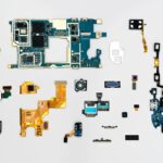
Printed Circuit Boards (PCBs) serve as the backbone of almost all electronic devices, acting as the essential platform upon which components are mounted. They're composed of a non-conductive substrate, usually made of fiberglass, layered with conductive pathways or traces that connect various components like resistors, capacitors, and integrated circuits.
- Key Functions:
- Electrical interconnection
- Structural support
- Thermal management
History of PCBs
The journey of PCBs dates back to the early 20th century when inventions like the radio and telephone demanded better component connections. By the 1940s, the concept evolved, leading to the first commercially manufactured PCBs.
- Timeline:
- 1936: The first PCB is patented.
- 1943: Production begins during World War II.
- 1960s: Widespread adoption in consumer electronics.
Reflecting on PCB history reminds us of how essential they’ve become in innovations over the decades, paralleling personal experiences with evolving technologies like smartphones and laptops.
Importance of Proper PCB Design
Functionality
Proper PCB design is pivotal for ensuring the functionality of electronic devices. A well-designed PCB optimally routes signals, reducing interference and maximizing performance. Imagine designing a high-fidelity audio device; every trace placement can enhance or degrade sound quality significantly.
- Key Aspects of Functionality:
- Efficient signal routing
- Minimization of electromagnetic interference
- Component accessibility for repairs
Reliability and Performance
Reliability in PCB design translates directly to a product’s longevity and effectiveness. A reliable PCB withstands environmental conditions and electrical stress without failure. Having dealt with electronic devices failing unexpectedly, the importance of robust designs becomes clear.
- Factors Influencing Reliability:
- Proper materials selection
- Thermal management techniques
- Rigorous testing procedures
Ultimately, careful attention to design ensures products perform consistently over time, providing peace of mind for both manufacturers and users.
Types of PCBs
Single-Sided PCBs
Single-sided PCBs are the simplest form of circuit boards, featuring components placed on one side with traces on the other. These PCBs are cost-effective and relatively easy to manufacture, making them popular for basic applications like calculators and simple gadgets.
- Advantages:
- Lower production costs
- Simplified design and manufacturing process
- Suitable for less complex electronics
Multi-Layer PCBs
In contrast, multi-layer PCBs incorporate multiple layers of conductive pathways, enabling more complex designs. These boards are essential in devices requiring advanced functionality, such as smartphones and computers.
- Benefits of Multi-Layer PCBs:
- Higher density of components
- Improved signal integrity
- Enhanced performance in compact spaces
Reflecting on personal experiences, utilizing multi-layer PCBs can transform an average device into a high-performance piece of technology, showcasing how the choice of PCB type can significantly impact overall product quality.
Key Components of PCB Design
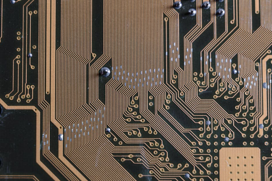
Traces and Pads
In PCB design, traces are the conductive pathways that connect different components, while pads serve as attachment points for these components. Think of traces as the roads that direct electronic traffic, and pads as the "parking spots" where parts are secured.
- Characteristics of Traces and Pads:
- Casually designed based on current requirements
- Different widths for various functions
- Strategically placed to optimize space
Vias and Holes
Vias and holes are crucial for creating connections between different layers on multi-layer PCBs. Vias are plated-through holes that allow electrical signals to travel vertically, while non-plated holes can accommodate mounting hardware.
- Key Functions:
- Vias provide vertical electrical connections
- Holes allow for component mounting and cooling
- Placement affects overall layout and thermal management
Reflecting on past projects, improper planning of traces, pads, vias, and holes can lead to complicated issues, highlighting their vital role in ensuring PCB functionality and efficiency.
Design Software for PCBs
Overview of Design Tools
In today’s fast-paced tech environment, PCB design software has become essential for engineers and hobbyists alike. These tools allow users to create schematic diagrams, simulate circuit behavior, and design layouts efficiently. Imagine a digital workspace where ideas come to life in real-time, making the design process visually engaging and intuitive.
- Key Features to Look For:
- Intuitive user interface
- Simulation capabilities
- Extensive component libraries
Popular PCB Design Software
There are several PCB design software options that cater to different needs and skill levels. Some of the most widely used include:
- Altium Designer: A robust tool known for its comprehensive features and high-end capabilities.
- Eagle: Popular among hobbyists, offering an easy-to-use interface with affordability.
- KiCAD: Open-source software that’s gaining traction due to its powerful features without the price tag.
Reflecting on personal projects, selecting the right software can significantly streamline the design process and lead to innovative designs that push boundaries.
Considerations for PCB Layout
Component Placement
When designing a PCB, component placement is a critical aspect that can significantly influence both functionality and performance. Properly arranging components can reduce signal paths, enhance accessibility for repairs, and optimize thermal management. Picture designing a complex board where every millimeter counts—strategic placement makes all the difference.
- Best Practices for Component Placement:
- Group related components together
- Maintain appropriate spacing for heat dissipation
- Consider maintenance accessibility
Signal Integrity
Signal integrity involves maintaining the quality of electrical signals as they travel across the traces. Factors like trace length, width, and routing can profoundly affect performance. A poorly designed layout can lead to cross-talk and interference, reminiscent of a crowded room where voices overlap, making it hard to focus.
- Key Factors Influencing Signal Integrity:
- Trace impedance matching
- Controlled layer stacking in multilayer PCBs
- Minimizing loop area for sensitive signals
Reflecting on past experiences, attention to component placement and signal integrity not only enhances reliability but also saves time during troubleshooting down the line.
Prototyping and Testing PCBs
Prototyping Methods
Prototyping is a vital step in the PCB design process, allowing engineers to test their concepts before mass production. Various methods can be employed depending on budget and complexity. For instance, breadboarding offers a quick way to validate designs visually.
- Common Prototyping Methods:
- Breadboarding: Ideal for simpler circuits, enabling easy modifications.
- Rapid Prototyping: Using techniques like 3D printing to create test versions quickly.
- PCB Fab Services: Outsourcing to professional services for quick turnaround.
Testing Procedures
Testing is crucial in ensuring that a PCB meets design specifications and functions as intended. Systematic testing helps pinpoint issues before deployment, saving money and time in the long run.
- Key Testing Procedures:
- Functional Testing: Verifying that each component operates correctly.
- Environmental Testing: Assessing performance under various conditions like temperature and humidity.
- Electrical Testing: Ensuring signal integrity and checking for shorts or opens.
Reflecting on personal projects, rigorous prototyping and thorough testing can transform guesses into reliable, effective designs, fostering confidence in the final product.

PCB Manufacturing Process
PCB Fabrication
The PCB fabrication process is where designs come to life, transforming raw materials into functional circuit boards. This stage involves etching the copper layer to create the necessary traces and pads, and it can be a fascinating process to watch. For many engineers, seeing their designs emerge can feel like watching a blueprint turn into reality.
- Key Steps in PCB Fabrication:
- Material Selection: Choosing appropriate substrates like FR-4 or polyimide.
- Copper Layering: Applying and etching copper to form traces.
- Drilling: Creating vias and holes for component mounting.
Assembly Techniques
Once fabrication is complete, the assembly process begins, where components are soldered onto the PCB. The assembly phase can vary widely based on the complexity and scale of the project.
- Common Assembly Techniques:
- Through-Hole Technology (THT): Components with leads inserted through holes and soldered on the opposite side.
- Surface-Mount Technology (SMT): Components mounted directly onto the surface of the board, allowing for a more compact design.
- Automated Assembly: Utilizing machines for high-volume production to ensure consistency and efficiency.
Reflecting on past projects, mastering both fabrication and assembly techniques is vital for delivering high-quality PCBs that meet stringent performance standards and customer expectations.