

Introduction to PCB Design
Importance of PCBs in Electronics
Printed Circuit Boards (PCBs) play a crucial role in the world of electronics. They serve as the backbone of most electronic devices, providing electrical connections and mechanical support for components. Imagine your smartphone or laptop; without PCBs, they simply wouldn't function. The integration and miniaturization of technology we enjoy today are largely possible because of efficient PCB design. Some key points highlighting their importance include:
- Connectivity: PCBs connect various electronic components seamlessly.
- Durability: They are typically made from materials that withstand environmental stress.
- Efficiency: The layout of a PCB can significantly affect a device's performance.
Basics of PCB Design Process
The PCB design process is a structured journey of transforming an idea into a functional prototype. It starts with conceptualizing your circuit, followed by creating a schematic diagram that defines the connections between components. Personally, I remember the first time I designed a PCB; I was amazed at how a simple layout could lead to a working circuit. The basic steps in PCB design include:
- Schematic Design: Mapping out the circuit connections.
- Layout Design: Arranging components on the board and defining traces.
- Design Rule Check (DRC): Ensuring the design meets specified standards.
- Prototyping: Creating a physical board to test functionality.
This process emphasizes the importance of attention to detail, as a small oversight can lead to significant issues later on.
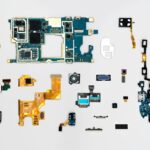
Understanding PCB Components
Types of PCBs
As we delve deeper into PCB design, it's essential to recognize the various types of PCBs, each tailored for specific applications. This was a revelation to me during my first projects; realizing that not all PCBs are created equal greatly influenced my designs. Here are some common types of PCBs:
- Single-Sided PCB: All components are placed on one side, suitable for simple circuits.
- Double-Sided PCB: Components are distributed on both sides, allowing for more complex layouts.
- Multilayer PCB: These boards consist of multiple layers, making them ideal for compact and high-performance devices.
Essential Components of Printed Circuit Boards
Diving into the essential components of PCBs, each plays a vital role in ensuring the circuit performs efficiently. My experience has taught me that understanding these components can prevent numerous headaches down the line. Some key components include:
- Resistors: Control current flow in the circuit.
- Capacitors: Store electrical energy temporarily.
- Diodes: Allow current to flow in one direction, protecting the circuit.
- Integrated Circuits (ICs): Serve as the brains of your circuit, integrating multiple functions.
Familiarity with these components not only enhances your design skills but also equips you to troubleshoot effectively when they arise.
Design Software and Tools for PCBs
Popular PCB Design Software
In the dynamic world of PCB design, the right software tools can make all the difference. Choosing the appropriate design software was one of the first decisions I faced, and it can be overwhelming with so many options available. Some of the most popular PCB design software include:
- Eagle: User-friendly platform for beginners and hobbyists.
- Altium Designer: A professional-grade tool with advanced features for complex designs.
- KiCad: An open-source option that is powerful and versatile.
- OrCAD: A robust software well-suited for electrical engineers.
Each of these programs offers unique features aimed at enhancing design efficiency.
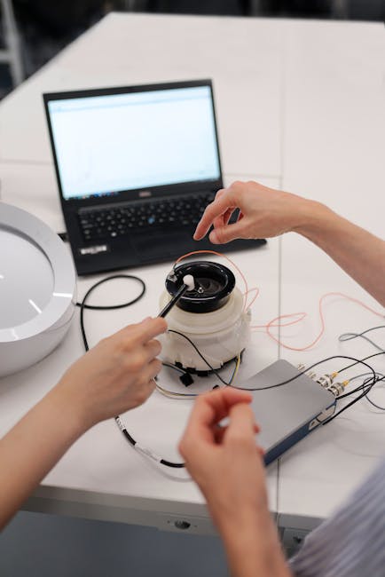
Tools and Equipment Needed for PCB Design
Beyond software, having the right tools and equipment is essential for successful PCB design. When I started, I was surprised by how critical these physical tools are in translating ideas into reality. Some essential tools and equipment include:
- Soldering Iron: For assembling and reworking the components on the board.
- Multimeter: To measure voltage, current, and resistance, ensuring components are functioning correctly.
- Oscilloscope: A valuable tool for observing the waveform of electronic signals.
- PCB Prototype Kit: Useful for testing designs before full-scale production.
Equipping yourself with these tools not only enhances your efficiency but also empowers you to iterate and improve your designs effectively.
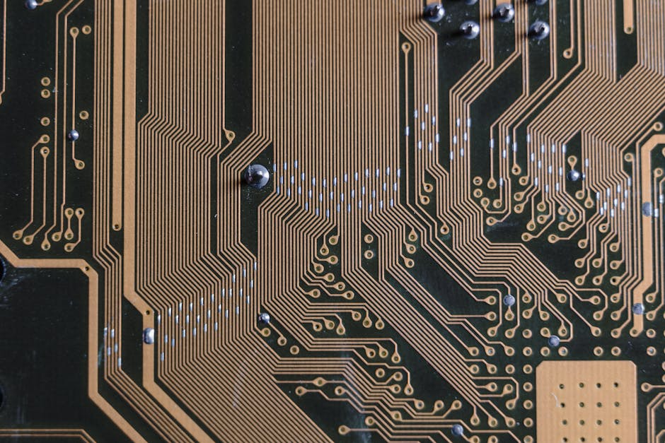
PCB Layout Design Guidelines
Key Considerations for PCB Layout
When it comes to laying out a PCB, there are several key considerations to keep in mind to ensure a successful design. From my own experience, addressing these factors early on can save a lot of time and headaches later. Some important aspects include:
- Component Placement: Arranging components logically reduces trace lengths and improves signal integrity.
- Layer Stack-Up: Decide on the number of layers based on complexity and space constraints.
- Ground Plane: Utilize a ground plane to minimize electromagnetic interference and improve stability.
- Thermal Management: Ensure there is adequate space for heat dissipation, especially near high-power components.
Best Practices for PCB Signal Routing
Once the layout is established, the routing of signals becomes crucial. I remember my initial struggles with signal routing, but adhering to a few best practices made a significant difference. Here are some of the best practices to follow:
- Keep Traces Short: This minimizes resistance and helps maintain signal integrity.
- Use Width Appropriately: Wider traces can handle more current, so adjust trace width based on current flow.
- Avoid 90-Degree Angles: Opt for rounded corners to reduce signal reflection and interference.
- Separate Analog and Digital Signals: Maintain distance between analog and digital traces to minimize noise.
By following these guidelines and best practices, designers can create effective PCBs that perform reliably and efficiently in their intended applications.
PCB Fabrication Process
Overview of PCB Fabrication Steps
Transitioning from design to fabrication is an exciting phase in the PCB development journey. I vividly recall my anticipation the first time I saw my design come to life. The fabrication process involves several key steps:
- Printing the Design: The initial design is printed onto a copper-clad board using photolithography.
- Etching: Unwanted copper is removed, leaving behind the desired circuit traces.
- Drilling: Holes for component leads and vias are drilled with precision.
- Plating: The board is plated to enhance connectivity and conductivity.
- Solder Mask Coating: A protective layer is applied to prevent solder bridging during assembly.
Each of these steps is crucial to ensure high-quality PCB production.
Factors Affecting PCB Manufacturing Cost
As with any manufacturing process, various factors can influence the cost of PCB production. Understanding these factors is vital for anyone involved in the design and manufacturing process. Some of the primary considerations include:
- Material Quality: Higher-grade materials can significantly increase costs.
- Layer Count: More layers usually mean higher complexity and cost.
- Quantity Ordered: Bulk orders typically reduce the per-unit cost.
- Lead Time: Rushed orders may incur additional fees.
By keeping these factors in mind, designers can better manage budgets and expectations throughout the PCB fabrication process.